
 English
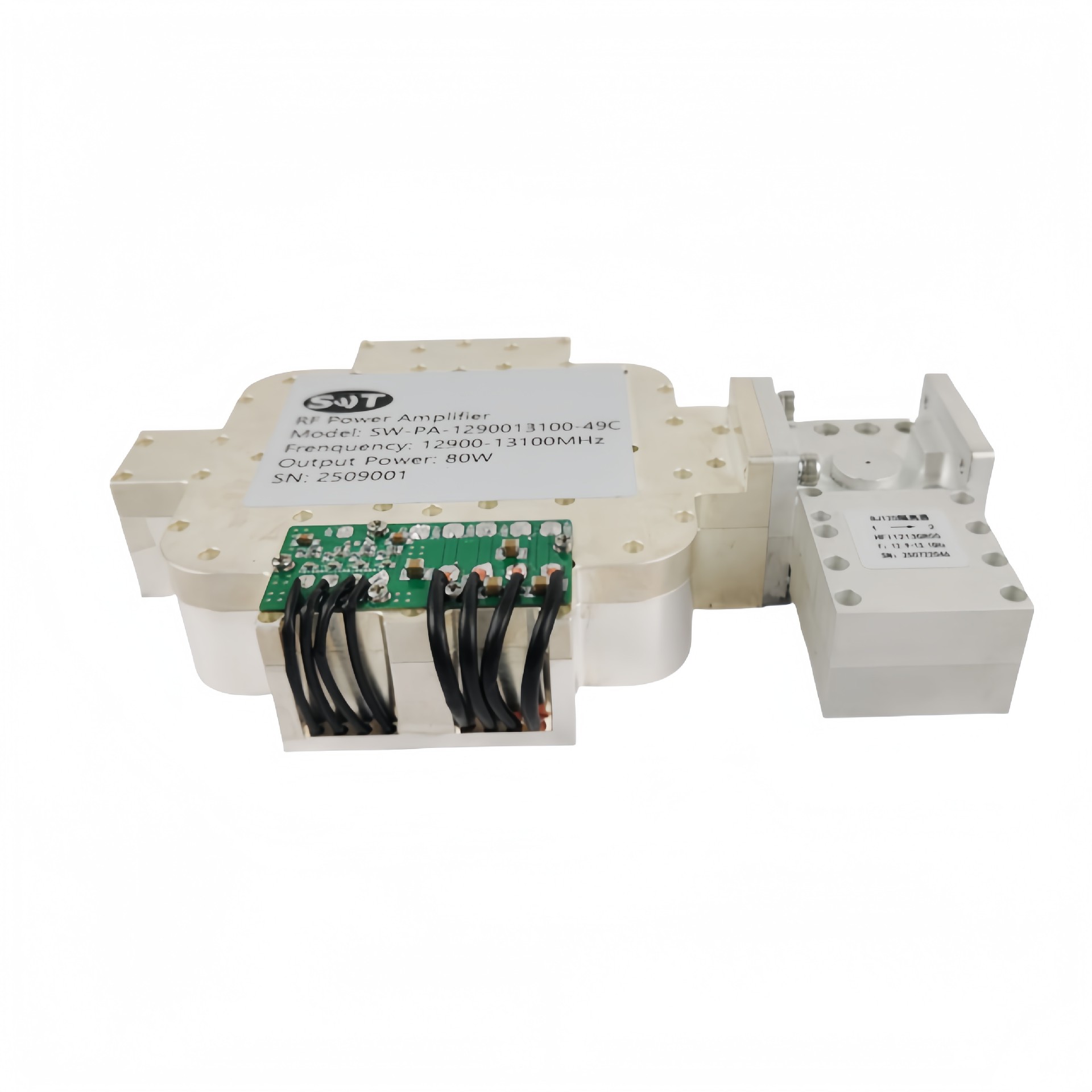
12.9-13.1 GHz 80W Power Amplifier for Industrial & Commercial RF Systems
Place of Origin:China
Brand Name:SWT
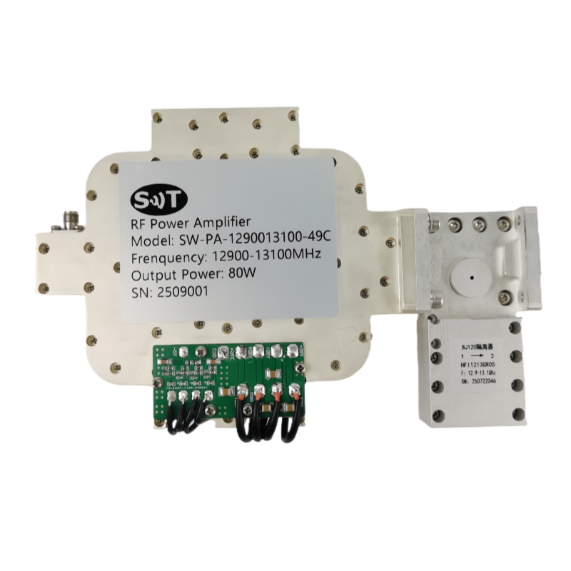
Model Number:SW-PA-1290013100-49C
Price:Please Contact Customer Service
Product Description
Description
The module is designed for both Industrial and commercial applications. The latest device technologies and design methods are employed to offer high power density, efficiency, and linearity in a small, lightweight package.
Specification
Typical performance at +28V DC +25oC, and in a 50Ω system.
RF / ELECTRICAL | ||||
PARAMETER | MIN | TYP. | MAX | UNIT |
Operating Frequency | 12.9 | 13.1 | GHz | |
RF INPUT | 0 | dBm | ||
Power Gain | 49 | dB | ||
P-1dB Output Power | 49 | dBm | ||
Power Gain temperature drift | 3 | dB | ||
In/Out Impedance | 50 | Ω | ||
Input VSWR | 1.3 | |||
Spurious Signals | -55 | dBc | ||
IMD3@Output 42dbm @ two tone space 5MHz | -25 | dBc | ||
Operating Voltage | 28 | V DC | ||
Power Dissipation | 700 | W | ||
MECHANICAL | ||
PARAMETER | VALUE | UNIT |
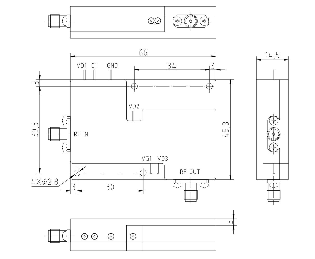
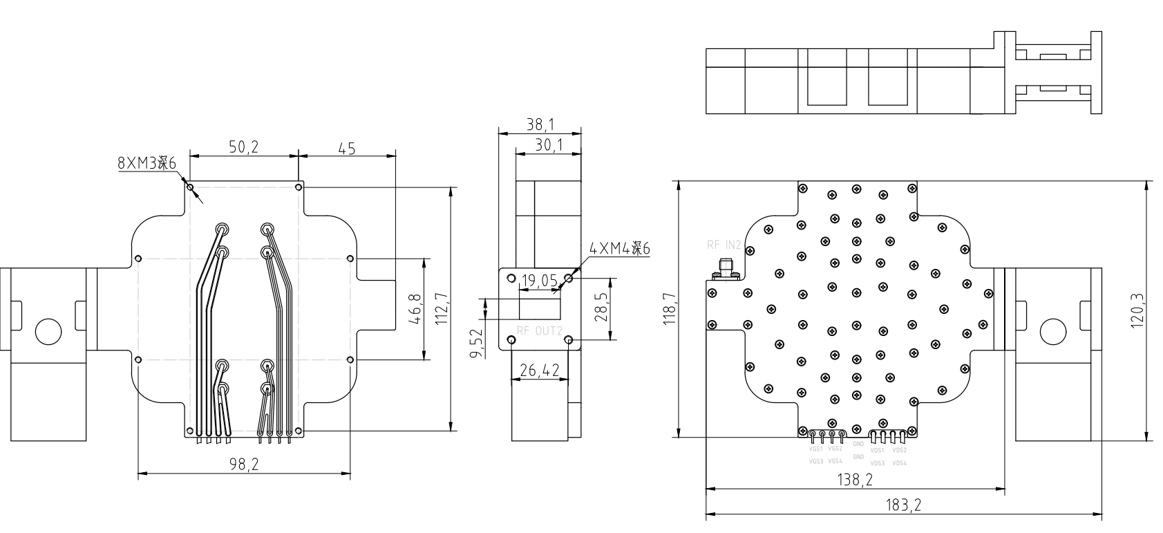
Dimensions (W x D x H) | 66*45.3*12 mm (SW-DRIPA-1290013100-31C) 183.2*120.3*38.1mm(SW-FINPA-1290013100-49C) | mm |
RF Connectors (Input / Output) | SMA-KF / WR75 (Flange BJ120) | -- |
Control Connector | Radio frequency powered insulator | -- |
Cooling | Forced air cooling for heat dissipation( A radiator needs to be installed.) | -- |
Weight | ≤8 | kg |
ENVIRONMENTAL / PROTECTIONS | |||
PARAMETER | MIN | MAX | UNIT |
Operating Temp. | 0 | +55 | °C |
Humidity Range | 0-100 | % | |
Amplifier Safeguard Temp. | +80 | °C | |
Protections | Output mismatch protection | ||
INPUT/OUTPUT panel Connector | |||
AMPLIFIER CONNECTOR TYPE: | —— | ||
TRIAD CABLE PART NUMBER: | —— | ||
NUMBER | interface type | DESCRIPTION | |
X1 | SMA-FK | RF IN1 | |
X2 | SMA-FK | RFOUT1 | |
X3 | SMA-FK | RFIN2 | |
X4 | WR75 | RFOUT2 | |
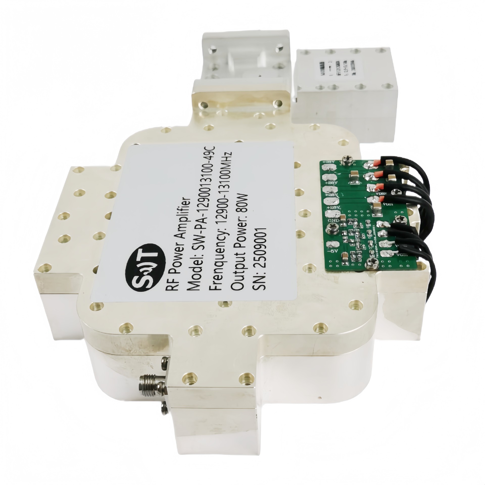
Connector Definition | ||
AMPLIFIER CONNECTOR TYPE: | ||
TRIAD CABLE PART NUMBER: | —— | |
NUMBER | Definition | DESCRIPTION |
Drive amplifica Drive amplification module (SW-DRIPA-1290013100-31C) | ||
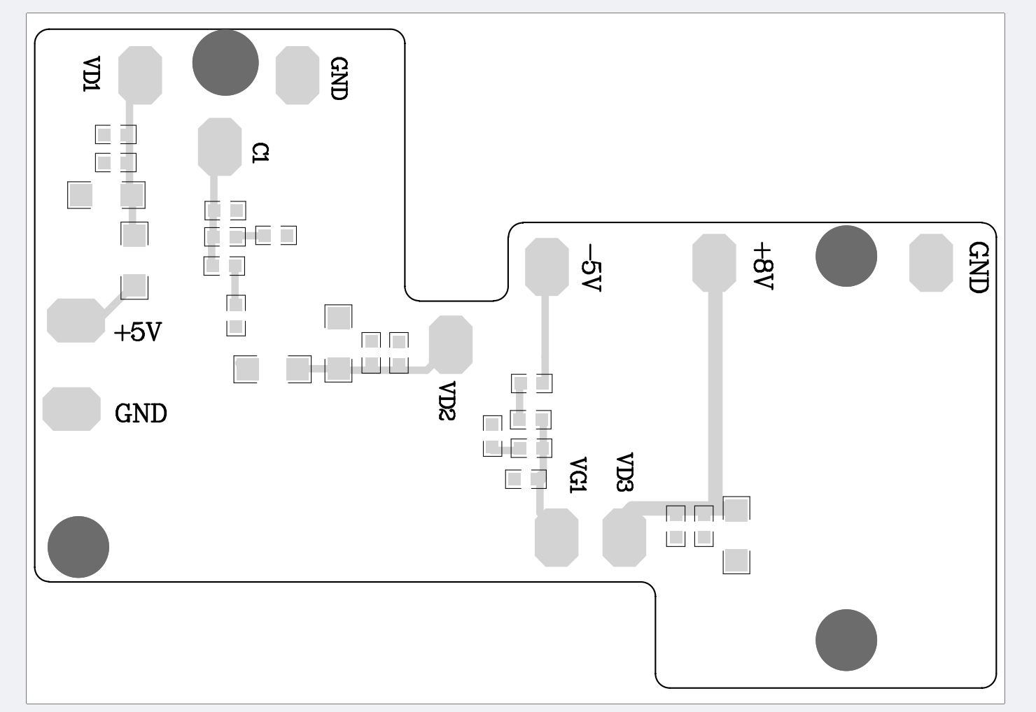
1 | VD1 | +3.5V (≤200mA) |
2 | C1 | +1.05V(≤100mA) |
3 | GND | GND |
4 | VD2 | +3.5V (≤200mA) |
5 | VG1 | -1V(≤100mA) |
6 | VD3 | +8V(≤1.8A) |
Final amplification module(SW-FINPA-1290013100-49C) | ||
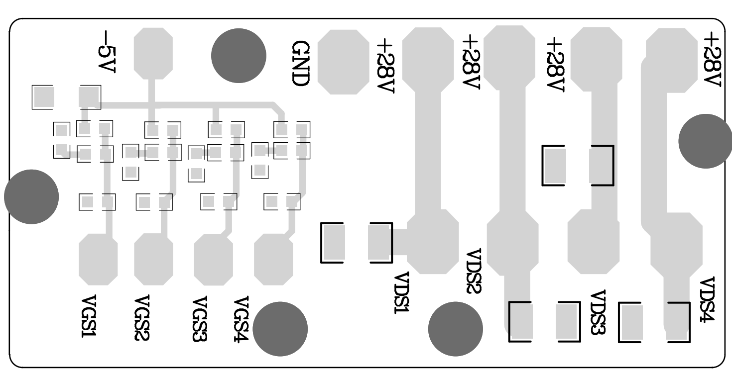
7 | VGS1 | -1.9V(≤100mA) |
8 | VGS2 | -1.9V(≤100mA) |
9 | VGS3 | -1.9V(≤100mA) |
10 | VGS4 | -1.9V(≤100mA) |
12 | VDS1 | +28V(≤6A) |
13 | VDS2 | +28V(≤6A) |
14 | VDS3 | +28V(≤6A) |
15 | VDS4 | +28V(≤6A) |
16 | GND | GND |
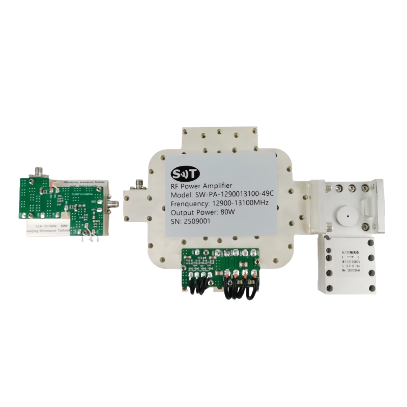
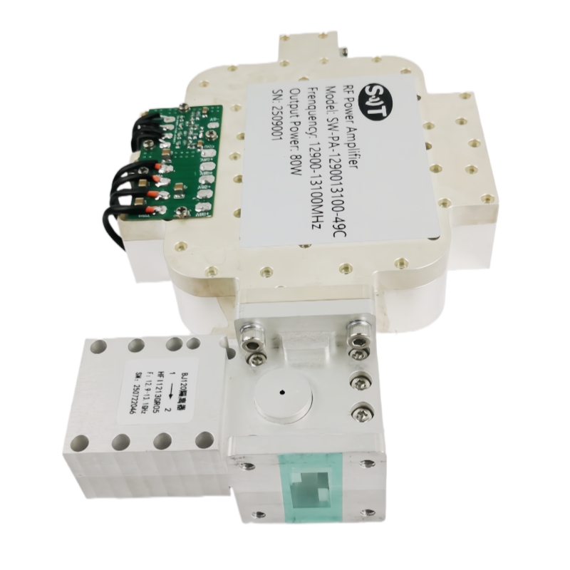
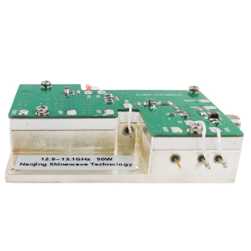
Drive amplification module (SW-DRIPA-1290013100-31C)
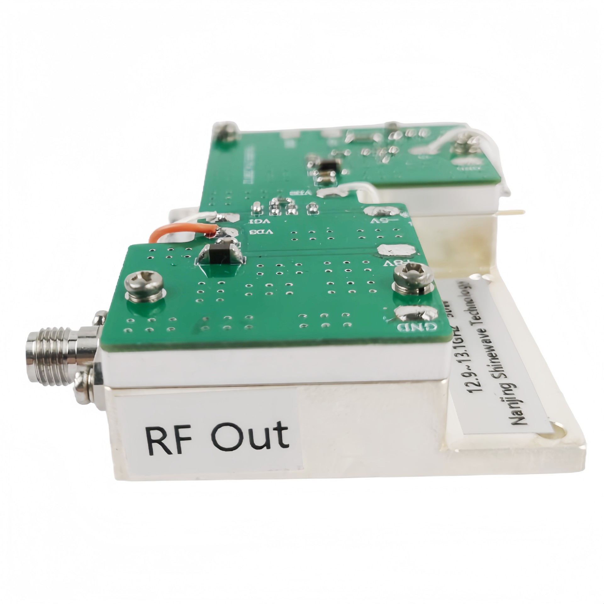
Cover plate installation PCB (SW-DRIPA-1290013100-31C)
Final amplification module(SW-FINPA-1290013100-49C)
Cover plate installation PCB (SW-FINPA-1290013100-49C)
Product Details
Name:
Operating Frequency:
Psat Output Power:
Gain:
Input Vswr:
Power Gain Flatness:
Spurious Signals:
Harmonic Signals:
Operating Temp:
Application:
Transport Package:
Specification:
Payment & Shipping Terms
Minimum Order Quantity
1/pcs
Packaging Details
Standard Packing
Delivery Time
5-8 work days
Payment Terms
L/C, D/A, D/P, T/T, Western Union, MoneyGram
Supply Ability
100pcs per month
Send Inquiry