
 English

Customized 4500-5000MHz 100W High Power RF Power Amplifier for Telecommunication
Place of Origin:China
Brand Name:SWT
Model Number:SW-PA-45005000-50C
Price:$5302/pcs
Product Description

Description
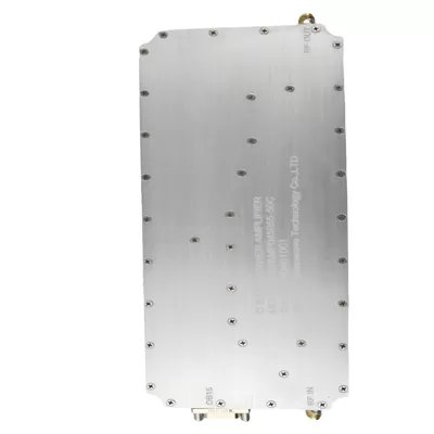
The C Band 4500-5000MHz 100W RF Power Amplifier is a specialized device designed to amplify radio frequency (RF) signals within the C Band frequency range, specifically from 4500 megahertz (MHz) to 5000MHz. Here's a detailed introduction to this RF power amplifier:
Frequency Range: This power amplifier operates within the C Band frequency range, covering frequencies from 4500MHz to 5000MHz. The C Band is commonly used in satellite communications, radar systems, and other high-frequency RF applications.
Power Output: The amplifier provides a power output of 100 watts, making it suitable for applications requiring high-power RF signals within the C Band.
Applications: The C Band 4500-5000MHz 100W RF Power Amplifier finds applications in satellite ground stations, radar systems, microwave links, point-to-point communications, and other C Band RF applications where high-power amplification is essential.
Performance: This amplifier is designed to deliver high-performance amplification while maintaining signal integrity and reliability. It ensures that amplified signals retain their quality and accuracy within the C Band frequency range.
Stability and Reliability: RF power amplifiers in the C Band are typically designed for stability and reliability, ensuring consistent performance in demanding environments.
Versatility: Despite its specific frequency range and power output, this amplifier can be integrated into diverse RF systems and setups that require high-power amplification within the C Band.
In summary, the C Band 4500-5000MHz 100W RF Power Amplifier is tailored for amplifying RF signals within the C Band frequency range. Its high-power output and performance characteristics make it suitable for various C Band RF applications, including satellite communications and radar systems.
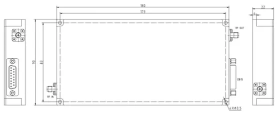
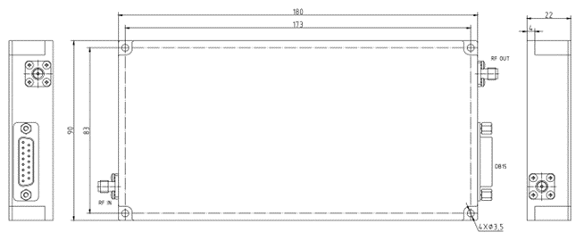
Outline Dimensional Drawing
Specification
Typical performance at +28V DC +25oC, and in a 50Ω system.
| RF / ELECTRICAL | ||||
| PARAMETER | MIN | TYP. | MAX | UNIT |
| Operating Frequency | 4.5 | 5 | GHz | |
| Input Power for Nominal Output | -15 | dBm | ||
| RF Input Maximum (peak) | -5 | dBm | ||
| Gain | 59 | dB | ||
| Output Power CW( peak RF input conditions at 4.75GHz) | 50 | dBm | ||
| Small Signal Gain Flatness | 3 | dB | ||
| P1dB | 44 | dBm | ||
| P3dB | 48 | dBm | ||
| PAPR | 6 | dB | ||
| ACPR(Harmonic Suppression) | -30 | dbc | ||
| Input Return Loss | 1.5:1 | 2.0:1 | ||
| Output Return Loss | 1.5:1 | 2.0:1 | ||
| Noise Figure(+25℃) | 7 | db | ||
| PAE | 30 | % | ||
| Impedance | 50 | Ohm | ||
| Voltage | 28 | V | ||
| MECHANICAL | ||
| PARAMETER | VALUE | UNIT |
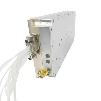
| Dimensions (L x W x H) | 180 x 90 x 22 | mm |
| RF Connectors (Input / Output) | SMA- KFD/ SMA- KFD | -- |
| DC Connector | DB15 | -- |
| Cooling | Consider heat dissipation with the system (Not Supplied) | |
| Mounting | φ3.5-4 Thru Hole | -- |
| Weight | ≤2 | kg |
| ENVIRONMENTAL / PROTECTIONS | |||
| PARAMETER | MIN | MAX | UNIT |
| Operating Temp. (Housing Temp.) | -40 | +60 | °C |
| Humidity Range | 0-100 | % | |
| PA Baseplate Shutoff Temperature | + 90 | °C | |
| TTL-level Enable | Enable Input should be drivable from GPIO of external controller | ||
| Forward Power | Status in DB15 connector | ||
| Reflected Power | Status in DB15 connector | ||
| Input Current | Status in DB15 connector | ||
| Device Temperature | Status in DB15 connector | ||
| INPUT/OUTPUT PINS | |||
| AMPLIFIER CONNECTOR TYPE: | DB15 | ||
| TRIAD CABLE PART NUMBER: | —— | ||
| PIN NUMBER | LABEL | DESCRIPTION | |
| 1 | VDD | +28Vdc IN | |
| 2 | VDD | +28Vdc IN | |
| 3 | VDD | +28Vdc IN | |
| 4 | VDD | +28Vdc IN | |
| 5 | GND | GROUND | |
| 6 | GND | GROUND | |
| 7 | GND | GROUND | |
| 8 | GND | GROUND | |
| 9 | DGND | DGND | |
| 10 | NC | NC | |
| 11 | On/Off | Amplifier Enable:TTL“HIGH (Logic 1) Amplifier Disable:TTL“LOW”(Logic 0) | |
| 12 | Forward Power | POWER DETECTOR (0-3.3V) | |
| 13 | Reflected Power | Reflected DETECTOR(0-3.3V) | |
| 14 | Input Current | Analog voltage relative to IDD@5A/V: IDD=0.14+5A*△V | |
| 15 | Device Temperature | Analog voltage relative to module temperature @10mv/℃:V=0.5+10mv*△℃ | |
Product Details
Name:
4500-5000MHz RF Power Amplifier
Operating Frequency:
4500-5000MHz
Psat Output Power:
100W
Gain:
59dB
Input Vswr:
2
Power Gain Flatness:
±3dB
Spurious Signals:
Harmonic Signals:
Operating Temp:
-40~60°c
Application:
Communication,EMC Test,Electronic Warfare
Transport Package:
Carton
Specification:
180 x 90 x 22mm
Payment & Shipping Terms
Minimum Order Quantity
1/pcs
Packaging Details
Standard Packing
Delivery Time
5-8 work days
Payment Terms
L/C, D/A, D/P, T/T, Western Union, MoneyGram
Supply Ability
100pcs per month
Send Inquiry