 English
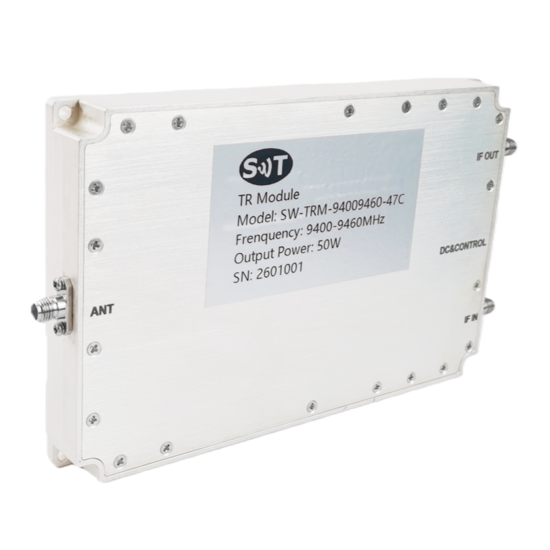
X band TRM Specification
Place of Origin:China
Brand Name:SWT
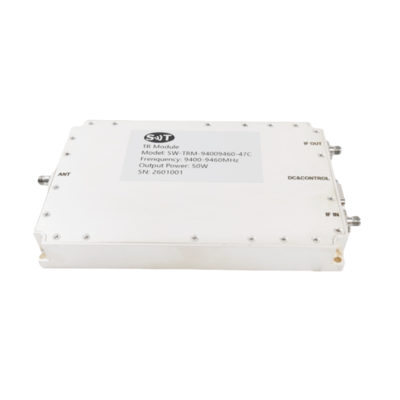
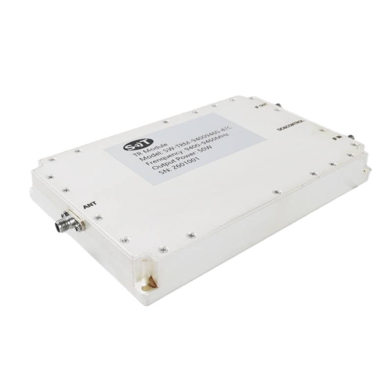
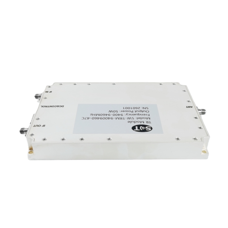
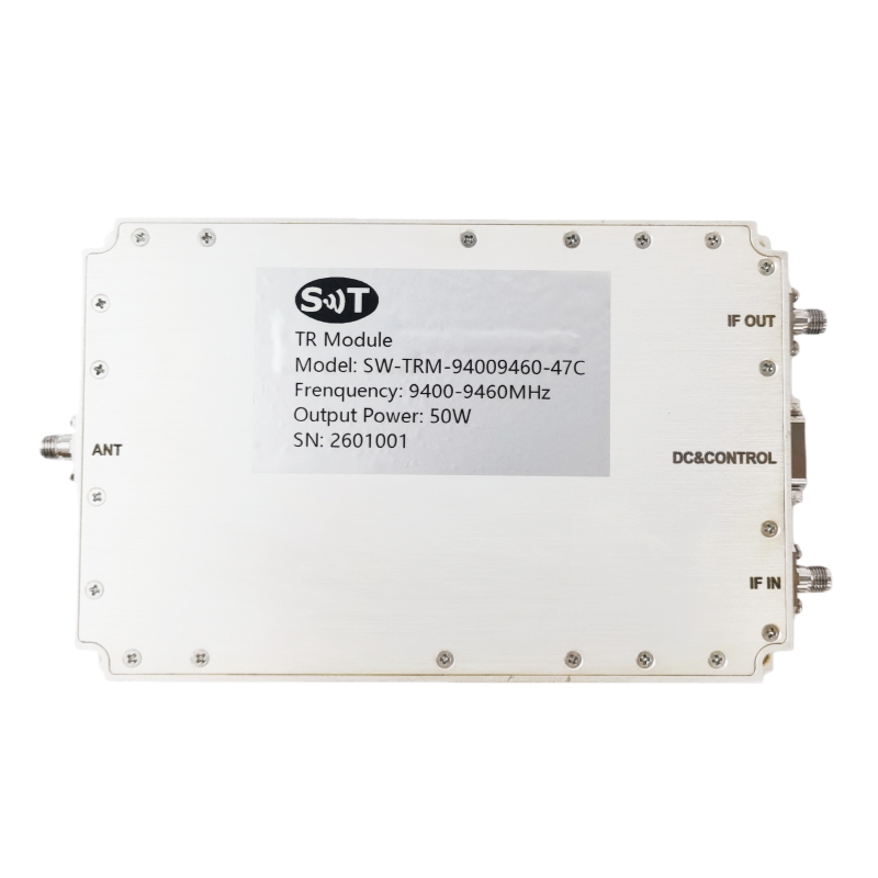
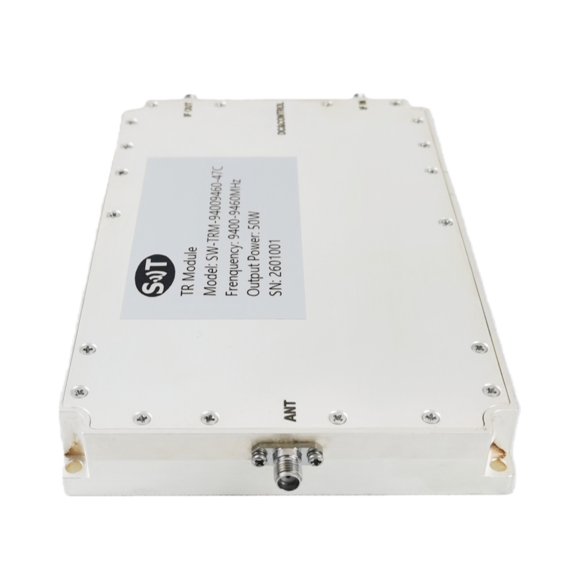
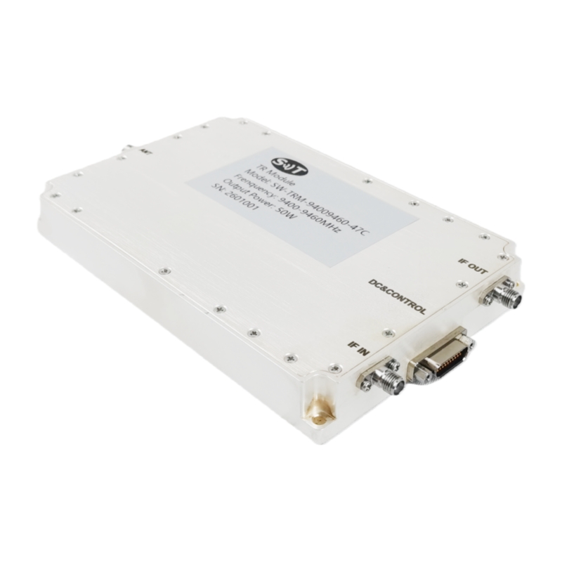
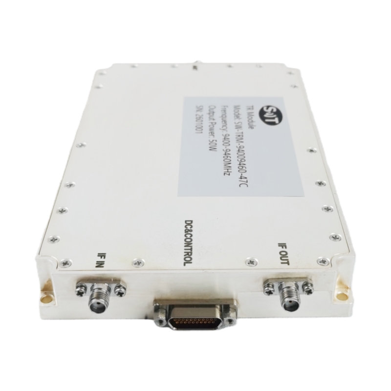
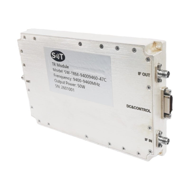
Model Number:SW-TRM-94009460-47C
Price:Please Contact Customer Service
Product Description
Description
TRM stands for Tx /Rx Module, the module consists of 01 TX/RX Channel, TRM controller, Health Monitoring and Power supply card. The TRM will have Tx input port、Tx output/RX input ports、 Rx output ports
Specification
Typical performance at +28V DC +25oC, and in a 50Ω system.
RF / ELECTRICAL | ||||||
PARAMETER | MIN | TYP. | MAX | UNIT | ||
Operating Frequency | 9400 | 9460 | MHz | |||
IF Filter Bandwidth of receiver 3dB | 60 | MHz | ||||
No. of Tx / Rx Channel | 1 | -- | ||||
Peak Output Power / Channel | 47 | dBm | ||||
Transmit Gain @ In all frequency/temps. | 47 | dB | ||||
Tx input Power | 0 | dBm | ||||
Second Harmonic of TX | < -25 | dBc | ||||
Pulse Width | 0..1 | 300 | us | |||
Max Duty Cycle | 25 | % | ||||
Pulse Droop | <0.5 (For 300 us pulse width) | dB | ||||
Fall Time | 100 | ns | ||||
Raise Time | 100 | ns | ||||
Transmit Channel Output ON/OFF Ratio | >110 | dBc | ||||
Power Added Efficiency | >25 % | |||||
VSWR (TX IN, ANT IN, RX OUT Ports) | 1.8:1 | -- | ||||
Rx Gain | 50 | dB | ||||
Rx Output P1dB | ≥10 | dBm | ||||
RX Input P1dB | -15 | dBm | ||||
Rx Noise Figure(0 dB | 3.5 | 4 | dB | |||
Rx Noise Figure(15 dB | 6 | dB | ||||
IF Filter Ripple | < 1 dB | Ripple in ±10Mhz around 75Mhz | ||||
Receiver Channel Image Rejection | >30 | dBc | ||||
Receiver Output in Band Spurious Rejection | >60 (Measured for +8 dBm output power) | dBc | ||||
Receiver Output Out of Band Spurious/Harmonics Rejection | >50 (Measured for +8 dBm output power) | dBc | ||||
Attenuator | 6 bits | 0~31.5 dB | ||||
Attenuator Accuracy | < 1.7 (RMS) | dB | ||||
Maximum Phase Change of Receiver Channel vs Attenuator States | <15° | 31.5 dB Attenuation State | ||||
Maximum Phase Change of Receiver Channel vs Attenuator States | <5° | 10 dB Attenuation State | ||||
LO Frequency | 9310 | MHz | ||||
Transmit Input to Receiver Output Isolation | >50 | dBc | ||||
Max. Rx tolerable power | ≥50W | Max duty cycle | ||||
Power Supply | 28 | V | ||||
Average currents | 1.75 @ DUC25% | A | ||||
Peaking currents | 7 | A | ||||
Protection against open output connector | Important, Design Guarantee | -- | ||||
Temperature reporting | Please use TMP36 IC for temperature (analog devices) | -- | ||||
MECHANICAL | ||
PARAMETER | VALUE | UNIT |
Dimensions (L x W x H) | 160 x 120 x 30 | mm |
RF Connectors (Input / Output) | SMA-K /SMA-K | -- |
DC /Control Connector | J30J – 21ZK | -- |
Weight | ≤1.5 | Kg |
ENVIRONMENTAL / PROTECTIONS | |||
PARAMETER | MIN | MAX | UNIT |
Operating Temp. (Housing Temp.) | -40 | +65 | °C |
Humidity Range | 0-100 | % | |
PA Baseplate Shutoff Temperature | + 80 | °C | |
Connector Definition | |
AMPLIFIER CONNECTOR TYPE: | J30J – 21ZK |
TRIAD CABLE PART NUMBER: | —— |
NUMBER | DESCRIPTION |
1,12,2,13 | +28V |
3,14,4,15 | GND |
5 | SEL (TTL 5v) |
16 | R (TTL 5v) |
6 | Load (TTL 5v) |
17 | T (TTL 5v) |
7 | Data (TTL 5v) |
18 | CLK (TTL 5v) |
8,9,19 | GND |
10 | Monitor voltage of Temperature |
21 | NC |
11,20 | NC |
Detailed info for power supply types as Table 2
Voltage | Limit Voltage (V) | Working Voltage Range (V) | Ripple wave (mV, ppm) | ||
min | max | min | max | ||
+28V | - | +29 | +27.5 | +28.5 | 100 |
TBD
Time Sequence and digital protcole
Serial data clock ‘CLOCK’ is the synchronous transmission clock of serial data ‘DATA’, TTL level is suggested to operate under 5MHz. Sampling the data at the falling edge of the CLOCK, with lower bits of the data in front and higher bits behind. Receive DATA at the falling edge of CLOCK and the shifting register operates correspondingly;Load the data of the shifting register to the buffer at the rising edge of LOAD.The serial data has 28 bits,with the low bit(Bit0) transmitted first and the high bit (Bit27) transmitted later.
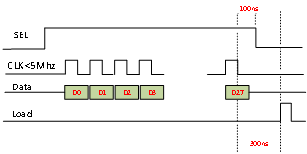
Fig. 1 Diagrams of the Serial control
When SEL is at high level, the signals of CLK、DATA、LOAD are valid. When SEL is at low level, block the signals of CLK and DATA and the serial data cannot be sent to the module. There are 28 bits data in the module. After generate falling edge after 28 CLK period (defined as one Data period) and upLoad the Data to the latch and output it.
Specific definition of one channel data is as shown below in the Table below:
Table 4 Definition for serial data
Order | Function | Remarks | ||
D0~D1 | Set 01 | 01 | ||
D2 | RX Standby Control | Low level standby, RX not working, High level,RX normal | ||
D3~D8 | Set 000000 | 000000 | ||
D9 | Rx ATT | Rx Attenuation Control | -0.5dB | High level valid IN IF |
D10 | Rx Attenuation Control | -1dB | ||
D11 | Rx Attenuation Control | -4dB | ||
D12 | Rx Attenuation Control | -16dB | ||
D13 | Rx Attenuation Control | -8dB | Low level valid IN RF | |
D14 | Rx Attenuation Control | -2dB | ||
D15 | TX ATT | Rx Attenuation Control | -0.5dB | High level valid |
D16 | Rx Attenuation Control | -1dB | ||
D17 | Rx Attenuation Control | -4dB | ||
D18 | Rx Attenuation Control | -16dB | ||
D19 | Rx Attenuation Control | -8dB | ||
D20 | Rx Attenuation Control | -2dB | ||
D21~D26 | Set 000000 | 000000 | ||
D27 | TX Stand by Control | Low level standby, Tx not working, High level,Tx normal |
Tx-En, are for activate or shut downing of Tx and Rx Path respectively and they are different form T and R signals. We determine it below:
Product Details
Packing:
Power Consumption:
Data Format:
Working Temperature:
Physical Interface:
Communication Interface:
Receiving Signal:
Applications:
Payment & Shipping Terms
Minimum Order Quantity
1/pcs
Packaging Details
Standard Packing
Delivery Time
5-8 work days
Payment Terms
L/C, D/A, D/P, T/T, Western Union, MoneyGram
Supply Ability
100pcs per month
Send Inquiry

ADD:Rooms 405 & 406, 4th Floor, Building 2, Big Data Industrial Base, No. 180 Software Avenue, Yuhuatai District, Nanjing, Jiangsu Province, China
+86 17302591509
+86-25-87702669
Contat Us
Copyright © 2026 Nanjing Shinewave Technology Co., Ltd. All Rights Reserved. PRIVACY POLICY